
WRAITH: NOT taping out a brick
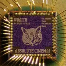
Okay, so I was supposed to write this post back in December, when I finished tapeout and the shuttle had been sent to TSMC. I got busy with other stuff (read lazy) and deferred it to now - when I am on summer break.
Before I get started, huge thanks to my teammates Ingi, Pradyun, and Sam without whom this project would not have been possible.
In this blog post, I essentially aim to casually summarize my work, if you want the technical report please read this.
What am I even talking about?
So early last year (2025), I had the opportunity to sign up for a super cool class labelled “Advanced VLSI and Tapeout” (go look at what other people did, it’s some epic stuff!!!). We get 1mm^2 of silicon (on TSMC’s 65nm node), and get pretty much free reign to do whatever we want. The course is sponsored by Apple, and the shuttle is handled by Muse Semi, a MPW (multi project wafer) company. Essentially, Muse will take a bunch of designs, all of which are too low volume for commercial production, plop them onto a single shared wafer, and then give that to TSMC to tapeout, batching low volume tapeouts together.
A bunch of my buddies were signing up for this class and I figured why not? It’s a cool opportunity and it’s pretty rare to get to be a part of every single stage in the silicon lifecycle (arch, RTL, DV, PD/PNR, DFT, si-val).
Usually, once you’re done with school and start working for “BIG” silicon, you get pigeonholed into working on one stage in this lifecycle - or so I’ve been told.
Everyone told me that this would be a gruelling experience, but I thought “How bad can it reaaaally be?”
It got pretty rough at times… but overall super awesome experience. Highly recommend it!
WRAITH
WRAITH, aka Workload Reconfigurable Array with Integrated Thread Handling, is a flavor of the CGRA architecture. A CGRA (coarse grain reconfigurable array) is a type of accelerator architecture that maps a bunch of hardware and data, to a “dataflow” graph. An easier way to think about it is like an FPGA, but instead of programming LUTs and how they connect to each other, you program “Processing elements” (think cores) and their interconnect. So if processing paradigms form a spectrum, it sits somewhere between a GPU and FPGA.
But when would you want a CGRA over a GPU or an FPGA? FPGAs take a while to program. Bitstreams take a while to compile and flashing usually requires a hardware reboot. CGRAs, because of their “coarse nature”, have considerably simpler bitstreams, and can be “reprogrammed” on the fly. This allows for more flexibility at runtime which is pretty neat! In theory, this also allows for self modifying kernels. Additionally, CGRAs offer power savings because you need less crossbar/interconnect area.
Unlike a regular CGRA, with statically scheduled dataflow, WRAITH’s mesh is reactive. No counters inside the PEs and no control logic. Packets contain metadata that determines routing and operations inside the mesh. I will detail more of the core architecture below.
Development
Background
So “ADRES” [1] (Architecture for Dynamically Reconfigurable Embedded Systems) was the starting point for us to consider architecture decisions. This architecture involves a system split into 2 components - a VLIW processor to handle instructions pertaining to control flow, and a Reconfigurable matrix that is responsible for executing dataflow kernels. Here “kernel” refers to the configuration that maps our dataflow graph to the grid of processing elements + the actual flow of data through it.
Often, flow charts for algorithms involve loops and other control structures. So there is significant compiler work required to “unroll” the loop and generate a configuration without control hazards. This is called “predicated execution” [2].
Architecture
Coming up with a block level overview of what we wanted to do, and a concrete architectural specification was the HARDEST part of this project. I had severely underestimated the amount of effort needed to create a robust architectural specification. In hindsight, this seems like a very obvious blunder, but at the time, I had never really architected a design with such limited constraints.
The Spec
Anywho, we decided to design a variation of the ADRES architecture. The key changes were:
- Replacing VLIW core with virtual frontends
- Instead of static routing, offer reconfigurable “routing tables” to each PE. The config in the routing table will tell the PE what to do to a packet (data + metadata) and where to send it next
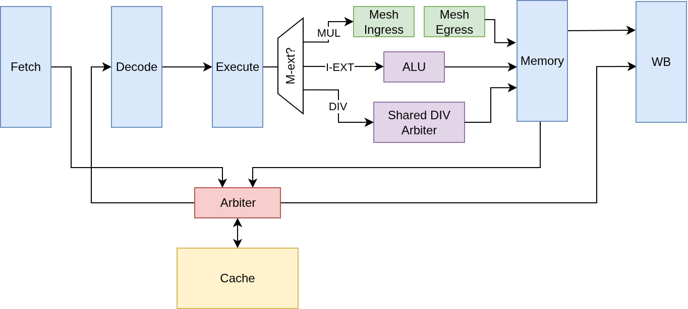
So instead of having a powerful VLIW processor along with the mesh, we use “virtual” cores instead, RVTUs (RISC-V Translation Units). Each RVTU is a full 5-stage RV32IM pipeline that executes ALU, branch, load, and store instructions natively. Multiplication is translated into packets and offloaded to the mesh for execution, and a shared 6-cycle divider handles division. The goal is for RVTUs to fill the role of e-cores while reusing the mesh hardware that would otherwise sit idle.
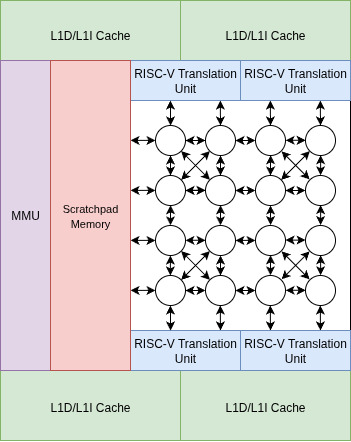
As for the mesh itself, we wanted to implement a 16x16 mesh of PEs. The mesh would be split into 4 clusters of 4x4 units. Each cluster would be fully connected, and clusters would connect 1-1 to their neighbors. We also planned for each cluster to have its own regfile, private to PEs in that cluster only.
This part of the spec was substantially larger and more ambitious than what we actually taped out. As area estimates got more realistic, we simplified the design until we landed on a 4x4 mesh containing 16 PEs with 2x2 subclusters.
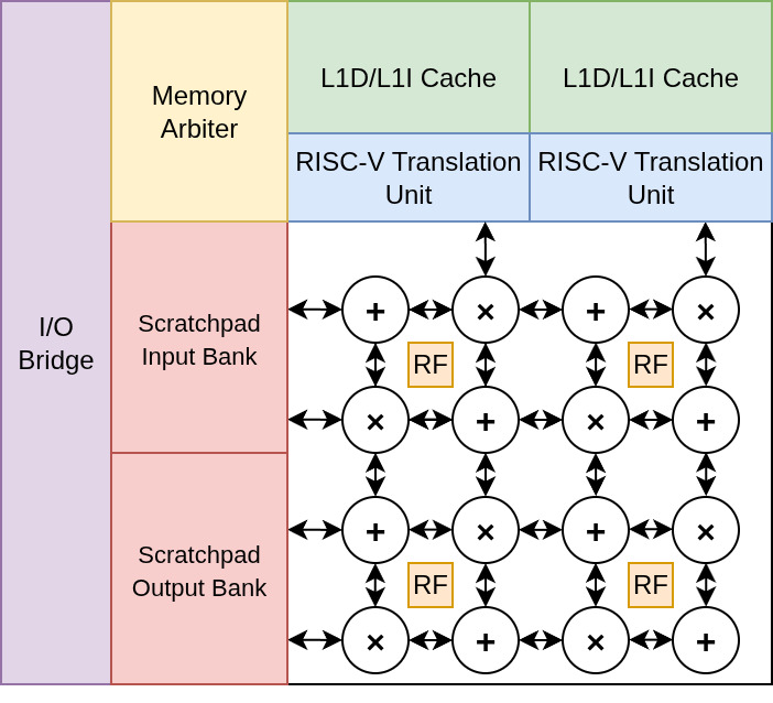
Each PE in the mesh would consist of an execution unit (either a multiplier or an ALU) and a routing table. The routing table is simply a hardware LUT that holds the mapping between packet id and routing actions. The ALU supports nearly the full RV32I operation set:
| fu_op | Operation | Description |
|---|---|---|
| 0 | a + b | Add |
| 1 | a << b | Shift left |
| 2 | a >>> b | Shift right (arithmetic) |
| 3 | a - b | Subtract |
| 4 | a ^ b | XOR |
| 5 | b | Pass-through (identity) |
| 6 | `a | b` |
| 7 | a & b | AND |
The only RV32I operations omitted are slt and srl.
Each packet in the mesh contains a Packet ID (PID) and a 32-bit value. When a packet arrives at a PE, the PID is used to index into the routing table (which we eventually called the Packet Action Table, or PAT). The PAT determines what operation should be performed, which register file entries should be accessed, and where the resulting packet should be sent next.
Packets follow the WIMP protocol (WRAITH Interconnect Mesh Protocol). Each WIMP packet is a single-beat message with two fields: a 4-bit PID and a 32-bit immediate.
Each PAT entry uses the following bitfield layout:
| Field | Width | Description |
|---|---|---|
| response_pid | 4 | PID for the output packet |
| dest | 3 | Output direction (includes SINK to terminate) |
| src | 5 | Register file index for input value |
| rd | 5 | Register file index for output write |
| rf_we | 1 | Register file write enable |
| imm_we | 1 | Write packet immediate directly to RF |
| src_imm | 1 | Interpret src field as an immediate |
| fu_op | 3 | Function select for the ALU/multiplier |
The dest field is 3 bits (not 2) to accommodate a SINK direction that terminates a packet with a side effect but produces no output, useful for spacer packets and RVTU load-immediate operations.
So if the PAT needs to be programmed before PEs can be routed, how do you program the PAT on reset? To deal with this, we reserved PIDs 0 and 1 for hardcoded routing, bypassing the PAT. As such these were used for programming the mesh.
Packets enter at the top-left node, traverse right until the correct column, then downward until they reach the destination PE. PID 0 allocates PAT entries (the packet immediate encodes the PAT write), and PID 1 loads constants into register files.
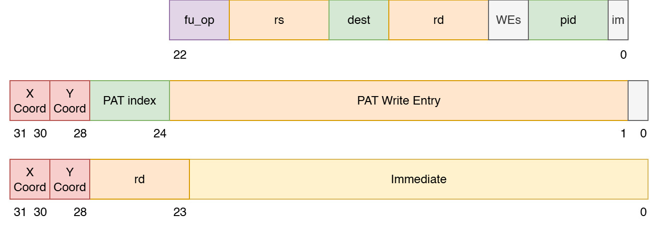
In this model, the mesh is completely reactive. There are no program counters sitting inside the PEs. Nothing happens unless a packet shows up. Packet arrives, look up the PAT entry, do some work, generate a new packet, and send it on its way.
In addition, we decided to use a “Scratchpad” memory to use as a staging space for packets going in and out of the WRAITH mesh. We also had a bunch of CSRs (Control and Status Registers) implemented in a smaller CSRfile. The goal was to expose all of WRAITH as a Memory-Mapped device (Hopefully the transfers to/from scratchpad are handled via DMA so the actual host CPU doesn’t waste cycles reading/writing to it).
We split the scratchpad into 2kB banks, one for staging input packets, and one for staging output packets. This greatly simplified dealing with port contention.
Lastly, we decided to implement our own communication protocol to / from the chip. Due to the 1mm^2 area restriction, doing PCI was impossible. We didn’t want to do a serial protocol because of the excessive IO latency associated with serializing kernels/data. As such, the communication protocol we used was a bi-directional 32-bit cooperative protocol, and it was ONE OF THE biggest weaknesses of our project. The protocol defines 8 message types:
| Code | Message Type | Description |
|---|---|---|
| 2 | Scratchpad Memory Write | Write to scratchpad (kernel config or data) |
| 5 | CSR Write | Write a control/status register |
| 3 | CSR Read Request | Request to read a CSR value |
| 1 | Scratchpad Mem Writeback | Flush kernel output to off-chip host |
| 8 | Cacheline Read Request | Request cacheline contents from host memory |
| 6 | Cacheline Writeback | Write back dirty cacheline |
| 7 | CSR Read Response | Contains value of last requested CSR |
| 4 | Cacheline Read Response | Contains previously requested cacheline contents |
The bus design is inspired by PCI Legacy, reusing AD[31:0]-style multiplexed address/data lines. However, there are no explicit REQ#/GNT# signals, arbitration priority is predefined, so devices know their turn without handshaking. This saved pins but made the protocol fragile.
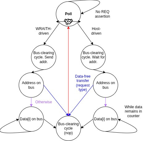
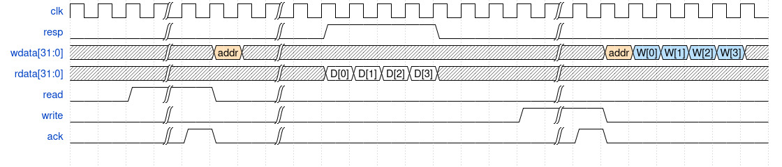
I have left out some of the details from this discussion (FIFOs, crossbars, etc) in order to (try to) keep the focus on what makes WRAITH interesting.
Timeline
So we had more or less figured out the architectural direction we wanted to go with by September 2025. The shuttle was due mid-November. That gave us ~2 months to do RTL, DV, PNR and all the final steps for handoff (LVS, DRC, etc). Also we had no one on our group with DFT experience, so we needed to spend some time figuring that out too.
(Side note: if you know of any good resources for learning more about DFT, please lmk!)
September
Spent most of the month writing RTL and doing block level DV
I ended up owning the RTL for the scratchpad memory, and the IO Bridge.
Because of the mesh specification being a bit hazy, the SPM block underwent 4 major design revisions. Writing the RTL was not too bad since it was essentially an ingress and egress FSM with some extra IO glued on top.
The IO bridge implemented the cooperative bus protocol. It was my first time developing HW that used tri-state buffers, so doing the verification for it was a bit challenging at first.
October
This is when I started doing a top-level verification harness. It was pretty fun and educational to write the massive
beast that top_tb was. I tried to do a good job utilizing some of the more “programming”-esque features of SV like fork join
and even synchronization constraints.
I was able to stick to a bunch of hierarchical components, which made a lot of my tasks for either generating stimulus, or driving stimulus fairly reusable. I ended up implementing a lock to model contention for the bus, and then spawned a bunch of threads that would attempt to grab the lock and use it to test IO transactions to/from the chip. There were some fairness issues, the cacheline-handler tasks always won arbitration and starved the polling tasks that checked mesh completion via CSRs, but those were fixed by adding a random 1–64 cycle wait to the cacheline handler’s main loop.
By the end of the month, the rest of the team had finished with the first pass of a post-synthesis post-pnr netlist, so we could start re-running verification with a back annotated SDF (standard delay format) file . An SDF basically tells the verification tooling what the skew/delay associated with each net is. That way you can actually test your chip with the timing constraints enforced by layout to make sure there are no weird skew/timing bugs in your design.
This second pass of testing was a lot easier thanks to the reusable components from the original testbench. All I really had to do was sub out a couple hierarchical references to some nets.
Post-PnR did expose a few ‘gotchas’ with SystemVerilog’s wait keyword.
Turns out VCS evaluates wait against pre-NBA signal values,
causing the testbench to follow an incorrect flow. A fixed-delay hotfix didn’t work due to metastability in FSM state registers, making this a bit annoying to fix.
November
Woohoo! We were done designing all of the chip! And we had passed verification!
We tried to do scanchain but it fried the timing on a lot of the blocks. So we elected to create a monstrous IO bridge bypass as our DFT hail mary. This led to having 6 dedicated pins that stream packets directly in and out of the compute mesh, bypassing the scratchpad and IO bridge entirely. It uses a rudimentary serialization protocol. We called it the “fallback”, but we didn’t have to end up falling back on it.
Actually, while working on this, we found a critical bug in the IO bridge at the last moment. Consequently, we had to redesign the co-operative FSM and reimplement/verify the bridge in the 24 hours leading to the trial shuttle deadline 🫠.
I wasn’t very familiar with innovus, LVS, STA, or clock-tree synthesis. Basically the tools that convert the post-PnR netlist into a GDSII file. So, I was able to take it relatively easy leading up to the shuttle. In hindsight, I should have tried to learn more about that part of the flow.
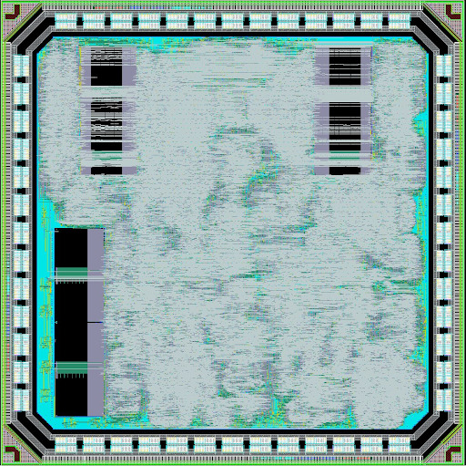
And lo, behold! The chip was shuttled successfully to TSMC. We would get them back in February 2026.
Some stats
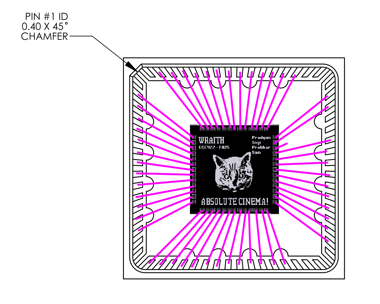
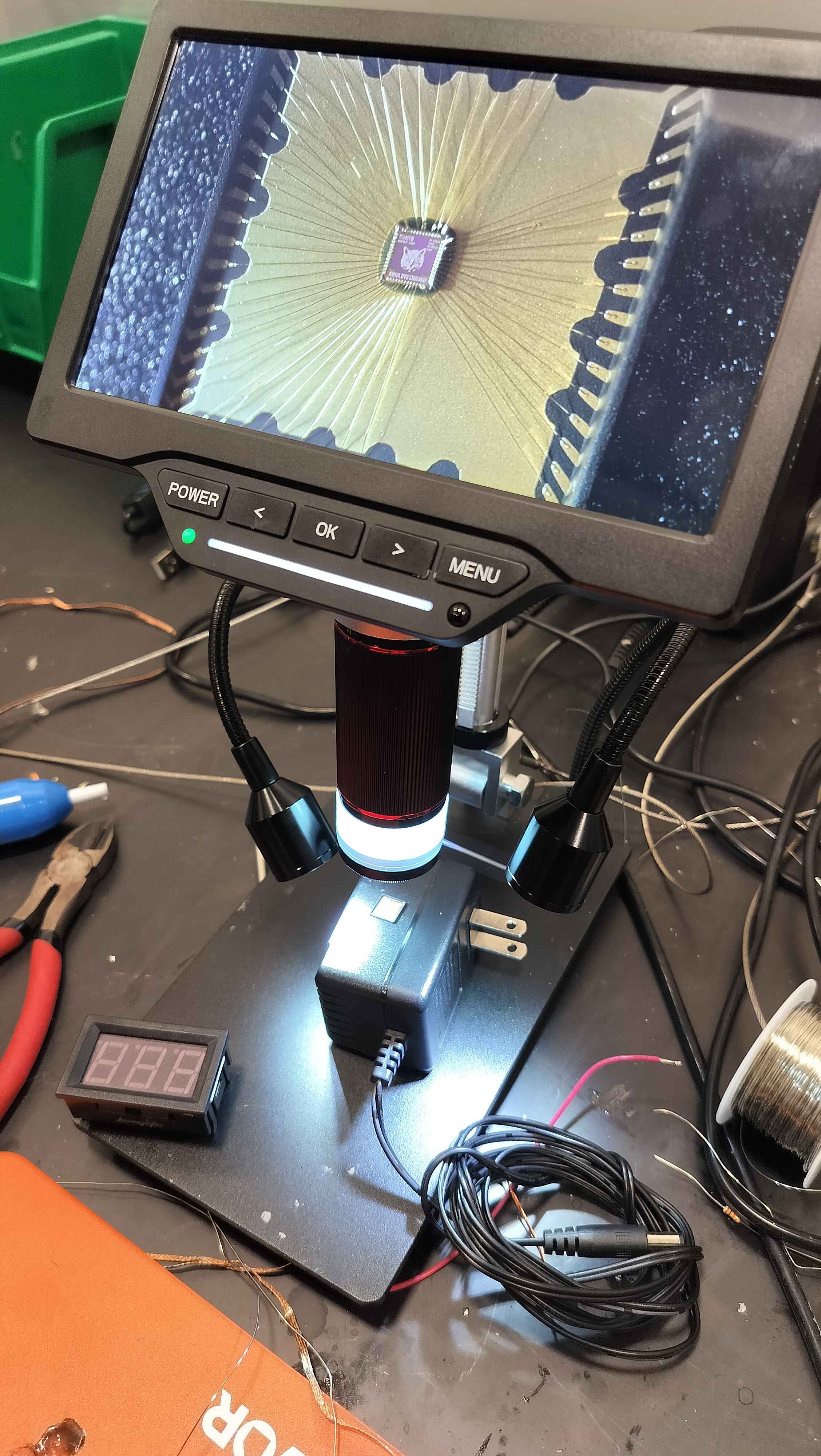
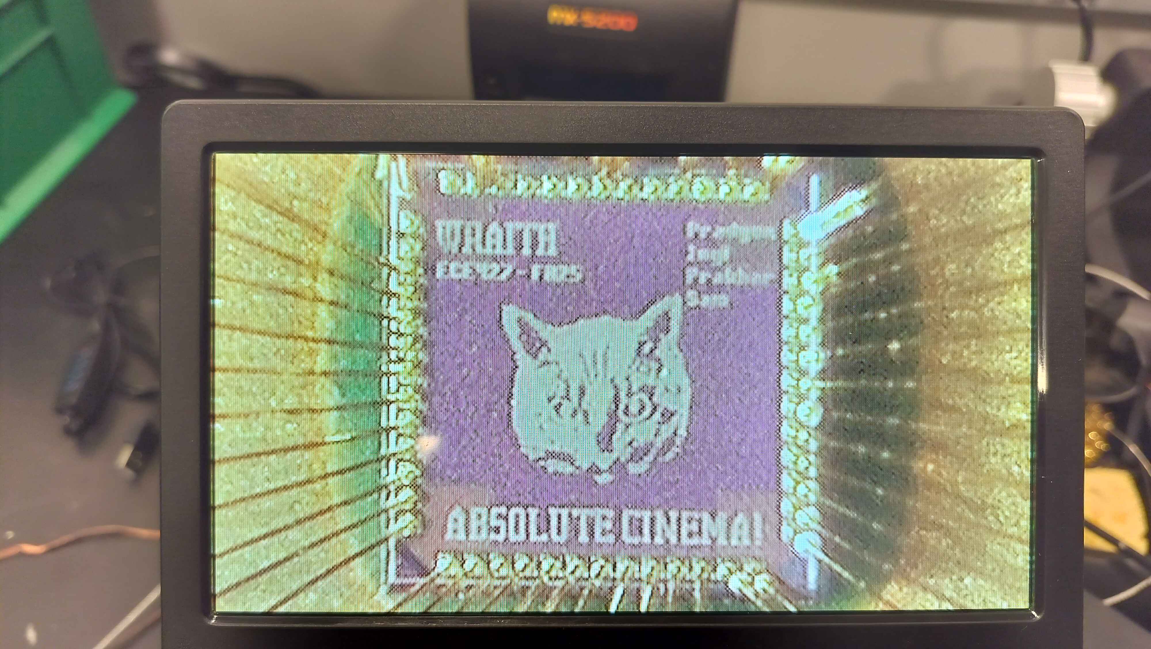
Our final chip is packaged in a QFN64 9mm package with a die size of 820×820µm and 77% core density (547,602µm² utilized out of 710,024µm² usable). It supports a theoretical maximum clock of 500MHz at 1.0V. Estimated power: 158.4mW internal, 122.9mW switching, and 255.2mW leakage (the register file IP reported a spurious 42W that we’re fairly confident is erroneous).
Bringup
(Warning: Incoming incoherent rambling)
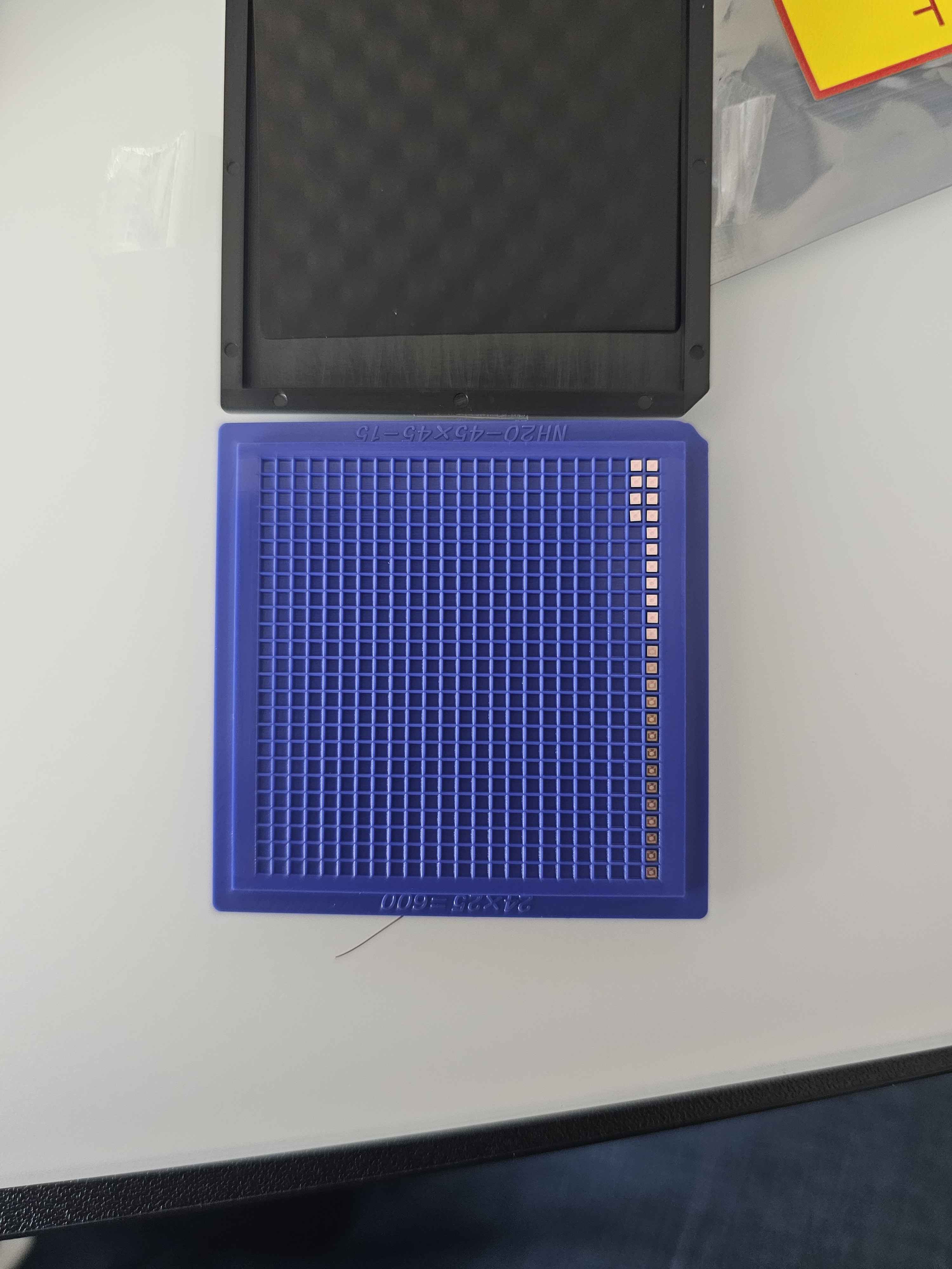
The chips arrived from the shuttle in February!
I LOVE AMD XILINX VIVADO on GNOME. Fun Fact: Every 5 implementations, Vivado will ask to screenshare? WHO IS Vivado sharing my screen to?? Turns out that vivado does this to prompt for feedback on their linux build? I am not entirely sure why they didn’t elect to just pop up a window instead.
We had access to some really neat development boards. To be precise, I got my hands on a VCU 118 eval kit.
These things cost ~15k USD a pop. I am very grateful that I got to use one for free.
Enter FMC - the FPGA Mezzanine Card Standard. This is a HS IO standard designed to support high-speed connections between FPGAs and daughter boards. The FMC standard supports 10Gbps, while FMC+ supports 28GBPs. The FMC connector is a BGA full of differential pairs.
Our chip uses 52 IO pins: 32 for the tri-state bus, 2 for RVTU resets, 6 for the SPM fallback (DFT) mode, 3 for IO bridge FSM state inspection, 1 for power indication, 2 for clock and reset, and 6 for power/ground pairs.
No differential pairs.
So we did something jank. We routed single-ended signals from the FPGA into the FMC diff pairs (one signal per pair) and hoped that it would work.
For a moment, we also thought we needed bidirectional high-speed level shifters. It was a rough week and I seriously thought that bringup effort was doomed. After talking to Stanley, we came to the conclusion of overvolting the chip, which would reduce its overall lifespan, but would allow us to interface with the FPGA.
As for the PCB design, we underwent multiple revisions. The first time, the PCB didn’t have enough spacing (3w rule).
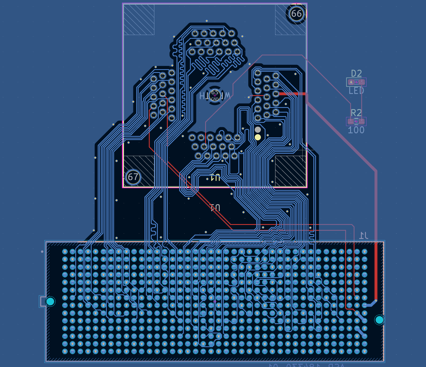
As for the second time, I wasn’t entirely satisfied with the mess I’d created.
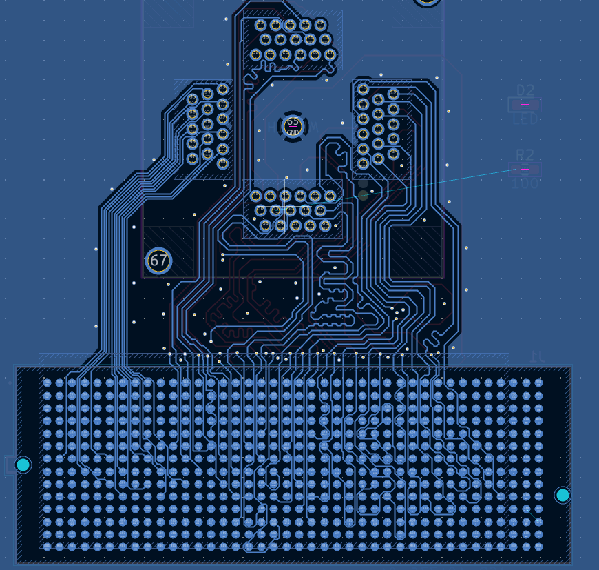
The third time was the charm, and I felt that the board was finally good enough! (
or maybe I just got too sick of using KiCAD xD)
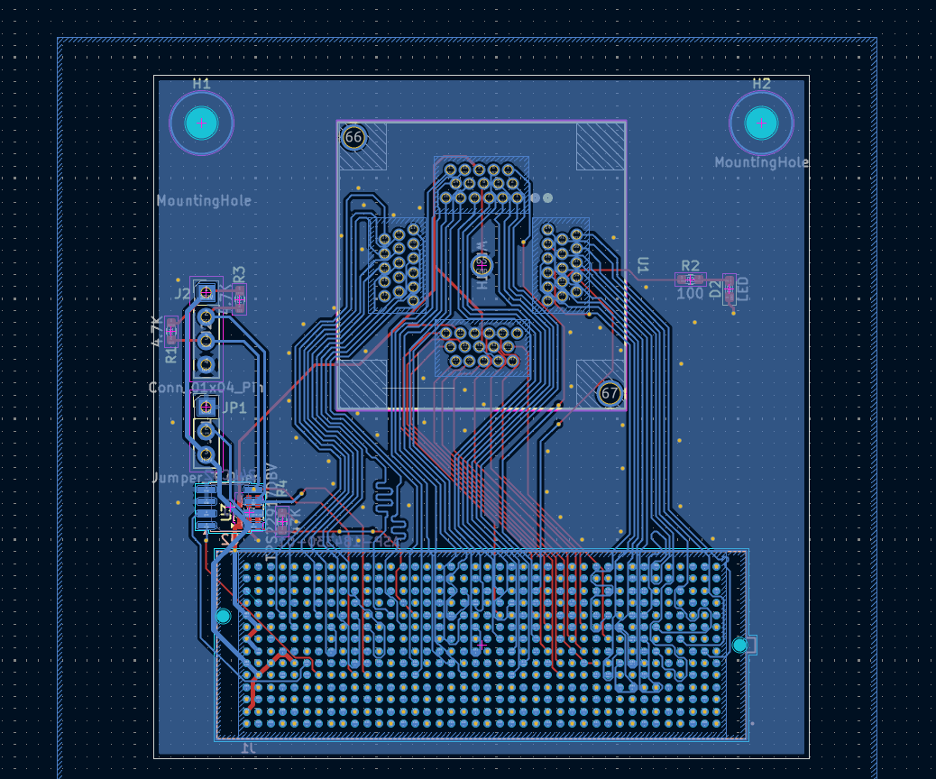
The final board used a 4-layer stackup with microstrip traces, an FMC+ connector, and a socketed chip. Bus and clock signals were length-matched to 56–61mm (~245ps for a 56mm trace) with 50Ω impedance control. The first manufactured board had the FMC+ connector installed backwards (READ your datasheet carefully!!!).
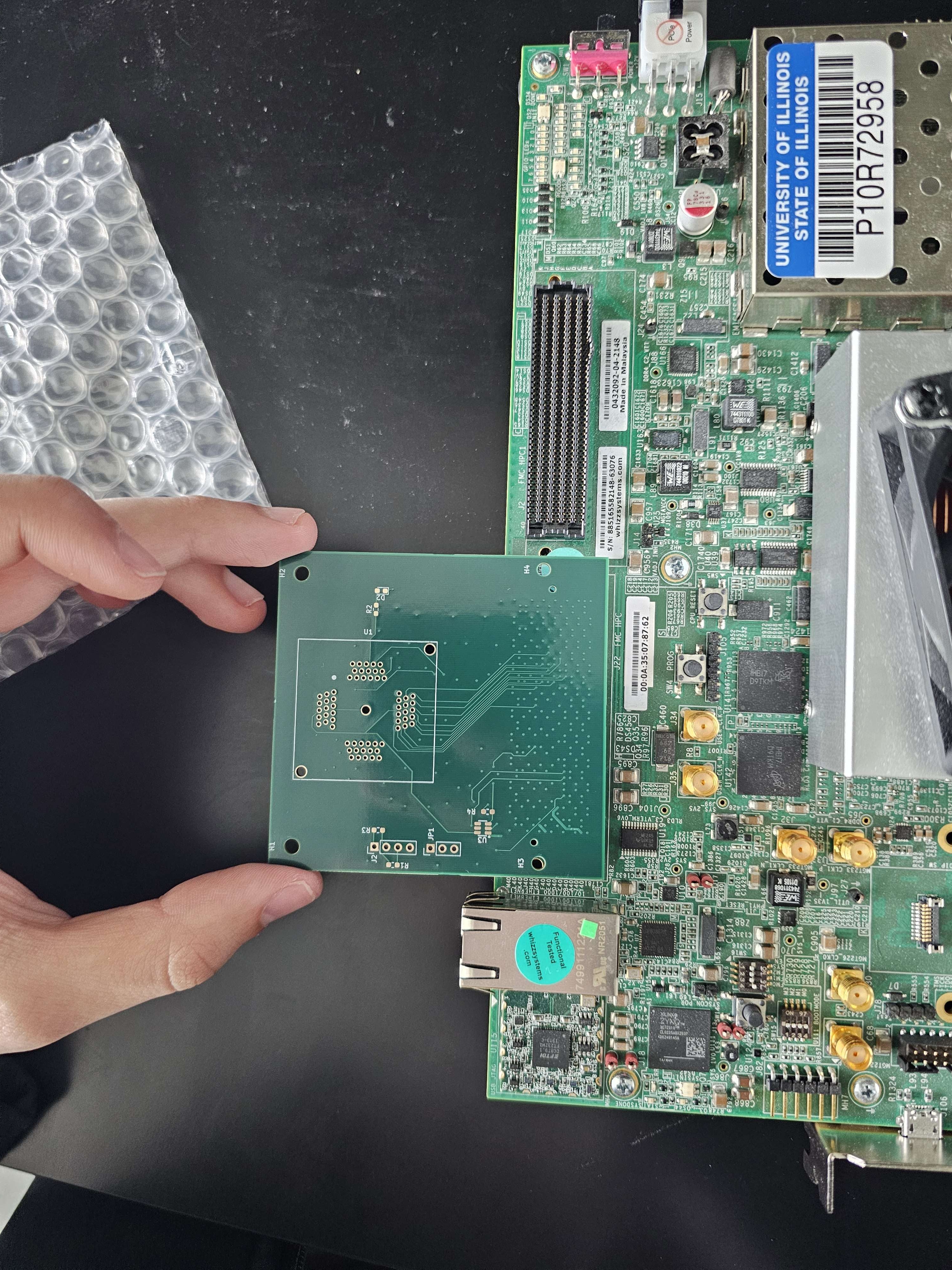
We couldn’t hit 250MHz because of timing constraints inside the FPGA. The VCU118’s “LA” bank splits across I/O banks 41 and 43, while the “HA” bank is in bank 70 on the opposite die corner. Routing between them added ~4ns of on-FPGA delay (compared to ~0.25ns for the PCB traces themselves), which capped testing at 125MHz at 1.8V.
Wrapping it up
All in all, working on this project was pretty fun. It did feel like a slog at times (I blame senioritis), but I learned so much knowledge that otherwise I would not have a reason to learn. We ended up winning the best project award from Apple (woohoo)!
References
[1] Mei, B., Berekovic, M., Mignolet, JY. (2007). ADRES & DRESC: Architecture and Compiler for Coarse-Grain Reconfigurable Processors. In: Vassiliadis, S., Soudris, D. (eds) Fine- and Coarse-Grain Reconfigurable Computing. Springer, Dordrecht. https://doi.org/10.1007/978-1-4020-6505-7_6
[2] https://en.wikipedia.org/wiki/Predication_(computer_architecture)